Serial Interface
Serial interfaces are typically used to connect the host-controllers to peripherals such as terminals and printers. The data (information) transfers in or out sequentially, one bit at a time using a single conductor, making it is a cost-effective interface.
GT-CP Serial Interface
One of three serial interfacing modes (UART, I2C, and SPI) can be selected via jumpers J5 and J6. For all modes, the SBUSY/ DTR signal reflects the receive buffer state, and the TRDY signal indicates if there is data currently held in the transmit buffer, so these signals can be used for flow control. All the data received is stored in the internal receive buffer and processed in the order it is recieved.
| J5 | J6 | Function |
|---|---|---|
| OPEN | OPEN | SPI mode |
| OPEN | SHORT | Factory Reserved |
| SHORT | OPEN | I2C mode |
| SHORT | SHORT | UART mode |
•Please refer to the respective hardware specification to confirm the jumper location
| Receive Buffer | 2,047 bytes |
|---|---|
| Transmit Buffer | 127 bytes |
| SBUSY Change | Interface | ‘L’(READY)→‘H’(BUSY) | ‘H’(BUSY) →‘L’(READY) |
|---|---|---|---|
| Receive buffer space | UART / I2C | 62 bytes or less | 128 bytes or more |
| SPI | 54 bytes or less |
| TRDY | READY(‘H’) | EMPTY(‘L’) |
|---|---|---|
| Condition | Data in transmit buffer | No data in transmit buffer |
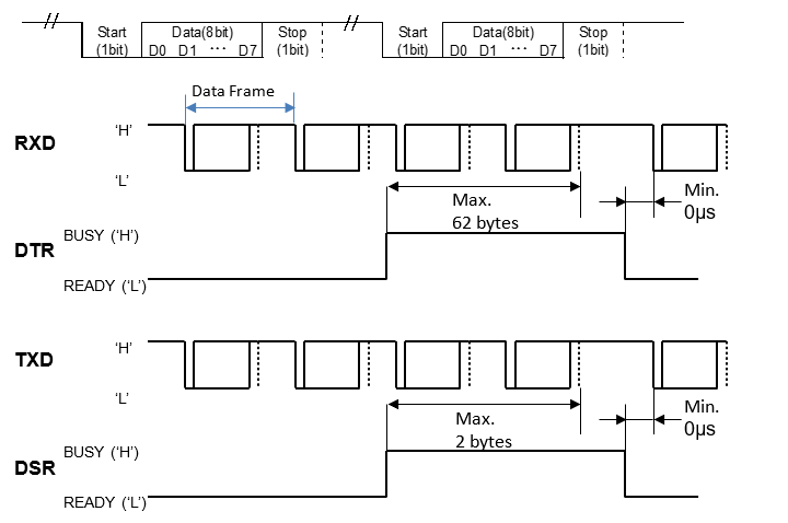
UART
Jumper selection
| J5 | J6 | Function |
|---|---|---|
| SHORT | SHORT | UART mode |
| J3 | J4 | Function |
|---|---|---|
| OPEN | OPEN | Set baud rate to 38,400 bps |
| OPEN | SHORT | Set baud rate to 19,200 bps |
| SHORT | OPEN | Set baud rate by memory switch setting |
| SHORT | SHORT | Set baud rate to 115,200 bps |
Refer to the software spec to see the memory switch setting details
Interface Pin Assignments
| Pin Number | Signal name | Function | Direction |
|---|---|---|---|
| 1 | /RESET | Hardware reset | Input |
| 2 | (Do not connect) | N/A | Input |
| 3 | RxD | Data receive | Input |
| 4 | DTR | Display busy | Output *1 |
| 5 | DSR | Host busy | Input |
| 6 | TxD | Data send | Output *1 |
| 7 | TRDY | Transmit ready | Output *1 |
| 8 | VCC | Power Supply (5V) | Input |
| 9 | GND | Ground | N/A |
Note *1: Output is high-impedance (Hi-Z) + pull-up resistor (53kΩ typ.) during power-on, reset input, and display internal initialization.
Note: Except for the Power supply, all the signals are 3.3V
Protocol
| Baud rate | 4,800 to 115,200bps (set by jumper and/or memory switch function) |
|---|---|
| Default setting: 38,400bps | Parity |
| None, even, odd (set by memory switch function) | Default setting: None |
| Format | Start (1 bit) + data (8 bit) + parity (0 or 1 bit) + stop (1 bit) |
| Communication Control Signal | DSR, DTR, TRDY |
•Data transmitted from the display is placed in the internal transmit buffer and sent, in order, when DSR = READY.
•TRDY signal does not need to be used.
Data Frame (With parity bit)

Data Frame (No parity bit)
SPI
Jumper selection
| J5 | J6 | Function |
|---|---|---|
| OPEN | OPEN | SPI mode |
Interface Pin Assignments
| Pin Number | Signal name | Function | Direction |
|---|---|---|---|
| 1 | /RESET | Hardware reset | Input |
| 2 | SCK | Serial clock | Input |
| 3 | MOSI | Data receive | Input |
| 4 | SBUSY | Display busy | Output *1 |
| 5 | SSEL | Host busy | Input |
| 6 | MISO | Data send | Output *1 |
| 7 | TRDY | Transmit ready | Output *1 |
| 8 | VCC | Power Supply (5V) | Input |
| 9 | GND | Ground | N/A |
Note *1: Output is high-impedance (Hi-Z) + pull-up resistor (53kΩ typ.) during power-on, reset input, and display internal initialization.
Note: Except for the Power supply, all the signals are 3.3V
Protocol
The display module operates as an SPI slave; data is sent and received in response to host (master) operations.
| 1st Byte | Operation Mode |
|---|---|
| 0x44 | Data write (Host → Module) |
| 0x54 | Data read (Host ← Module) |
| 0x58 | Status read (Host ← Module) |
| Baud Rate | Max. 8.3Mbps |
|---|---|
| Format | SPI |
| Communication Control Signals | SBUSY, TRDY |
•The TRDY signal may be monitored, but the host (master) must still use the Status Read sequence before the Data Read sequence.p>
•The SBUSY signal can be monitored directly or via the Status Read sequence.
Data Write
When 0x44 is input as the first byte, the module receives the 2nd and subsequent bytes as data.
| 1st byte | 2nd byte | 3rd byte | — | n+1 byte | |
|---|---|---|---|---|---|
| MOSI | 0x44 | Data(1) | Data(2) | — | Data(n) |
| MISO | – | – | – | — | – |
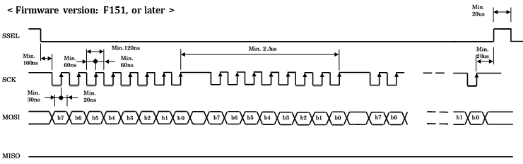
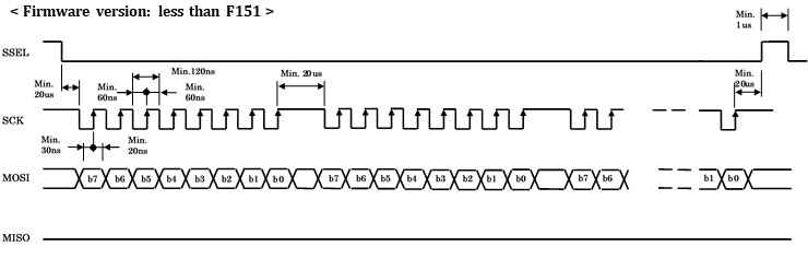
Data Write Timing
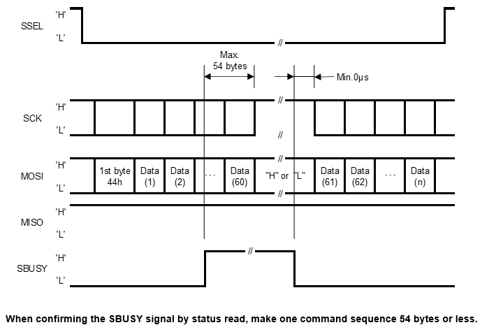
Data Write Timing Details
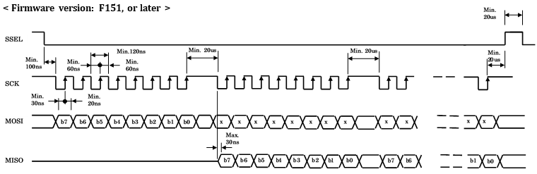
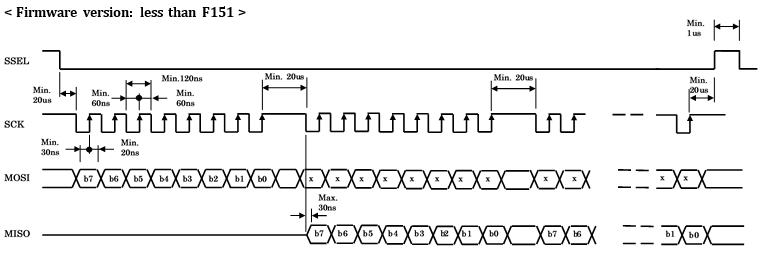
Data Read
When 0x54 is input as the first byte, the module outputs valid data on the 3rd and subsequent bytes. The host must read the number of bytes reported by the immediately preceding Status Read command. The number of bytes reported by the Status Read command will be transmitted, with any unread bytes discarded.
| 1st byte | 2nd byte | 3rd byte | — | m+2 byte | |
|---|---|---|---|---|---|
| MOSI | 0x54 | – | – | — | – |
| MISO | – | 0x00 | Data(1) | — | Data(m) |
m: The number of data bytes reported by the Status Read command(TL of status byte).
Status Read
When 0x58 is input as the first byte, the module outputs status data. For the 3rd and any subsequent bytes, the most recent status data is provided.
| 1st byte | 2nd byte | — | n byte | |
|---|---|---|---|---|
| MOSI | 0x58 | – | — | – |
| MISO | – | Status | Status | Status |
SBUSY: SBUSY signal
TL: Number of transmit data bytes available (maximum 63 bytes)
*: If b6 is 1, the status byte is invalid.
DaStatus and Data Read Timing
I2C
Jumper selection
| J5 | J6 | Function |
|---|---|---|
| SHORT | OPEN | I2C mode |
| J0 | J1 | Function |
|---|---|---|
| OPEN | OPEN | I2C slave address = 50h |
| OPEN | SHORT | I2C slave address = 51h |
| SHORT | OPEN | I2C slave address = 52h |
| SHORT | SHORT | I2C slave address = 53h |
Note: Module does not respond to the general call address (0x00).
Interface Pin Assignments
| Pin Number | Signal name | Function | Direction |
|---|---|---|---|
| 1 | /RESET | Hardware reset | Input |
| 2 | SCL | Serial clock | Input |
| 3 | SDA | Data receive | Input / Output |
| 4 | SBUSY | Display busy | Output *1 |
| 5 | (Do not connect) | N/A | Input |
| 6 | (Do not connect) | N/A | Output *1 |
| 7 | TRDY | Transmit ready | Output *1 |
| 8 | VCC | Power Supply (5V) | Input |
| 9 | GND | Ground | N/A |
Note *1: Output is high-impedance (Hi-Z) + pull-up resistor (53kΩ typ.) during power-on, reset input, and display internal initialization.
Note: Except for the Power supply, all the signals are 3.3V
Protocol
The display module operates as an SPI slave; data is sent and received in response to host (master) operations.
| Baud Rate | Max. 400kbps |
|---|---|
| Format | I2C |
| Slave Address | Set by jumper J0 and J1 (Default setting: 50h) |
| Supported Functions | ACK response, clock stretch |
| Communication Control Signals | SBUSY, TRDY, clock stretch |
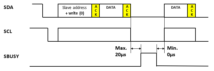
Note: If clock stretch is applied during processing of a command, the host (master) will not be able to send or receive any more data until command processing has finished.
If TRDY = EMPTY, 0xFF is transmitted from the module in response to a read sequence.
In addition to the clock stretch function, flow can also be controlled by monitoring the SBUSY signal. SBUSY signal changes according to the receive buffer state. The host should send data when SBUSY=READY.
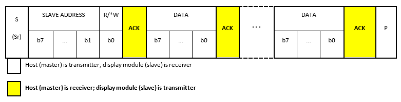
Data Write Sequence Frame
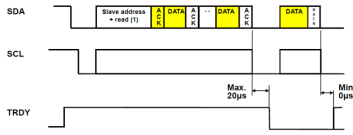
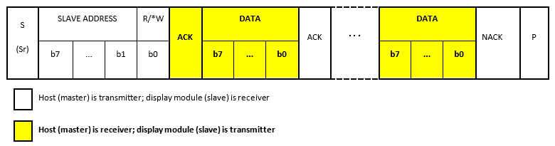
Data Read Sequence Frame
I2C Timing
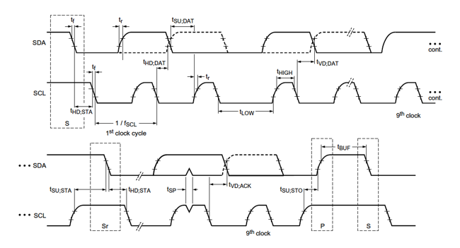
| Parameter | Symbol | Condition | Min. | Typ. | Max. | Unit |
|---|---|---|---|---|---|---|
| SCL clock frequency | fSCL | – | 0 | – | 400 | kHz |
| Start condition hold time | tHD;STA | – | 0.6 | – | – | µs |
| SCL ‘L’ time | tLOW | – | 1.3 | – | – | µs |
| SCL ‘H’ time | tHIGH | – | 0.6 | – | – | µs |
| Start condition setup time | tSU;STA | – | 0.6 | – | – | µs |
| Data hold time | tHD;DAT | – | 0 | – | – | µs |
| Data setup time | tSU;DAT | – | 100 | – | – | ns |
| SCL, SDA rise time | tr | – | 20 | – | 300 | ns |
| SCL, SDA fall time | tf | – | – | 300 | ns | |
| Stop condition setup time | tSU;STO | – | 0.6 | – | – | µs |
| Stop condition – start condition bus idle time | tBUF | – | 20 | – | – | µs |
Data Write Sequence
Data Read Sequence