
Thick Film Technology
Thick-film high precision pattern formation to align with Thin-film patterns
Noritake Thick-film Technology has been used in the VFD production process for a long time and enables high precision pattern formation aligned with Thin-film patterns.
We can also apply Photo-lithography technology to make even better accuracy patterning to the phosphors, insulators, etc.
We can supply high-quality Thick-film forming in the work area up to 500 x 350mm.
Please consult us with higher requirements.
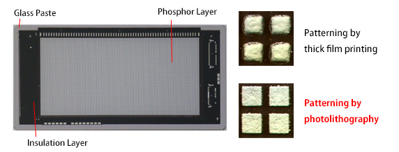
Example of Noritake Thick-film technology on the VFD glass substrate
| Photo-lithography | Dot Pitch | 325μm min. |
|---|---|---|
| Dot Size | ◻200μm min.* | |
| Tick Film Printing | Line Pitch | 500μm min. |
| Line Width | 200μm min. | |
| VIA hole | 60×150μm min(Hex shape) | |
| Printing Material | Conductive materials – Silver.etc Black insulator, Transparent insulator Glass paste, etc. |
|
| Substrate Material | Glass, Ceramics, etc. | |
| Applicable Work Size (area) | 500 x 350mm (Max.) | |
| Application in VFD | Display pattern, Insulation layer formation, etc. | |
*the square ◻
symbol means both side members are the same length